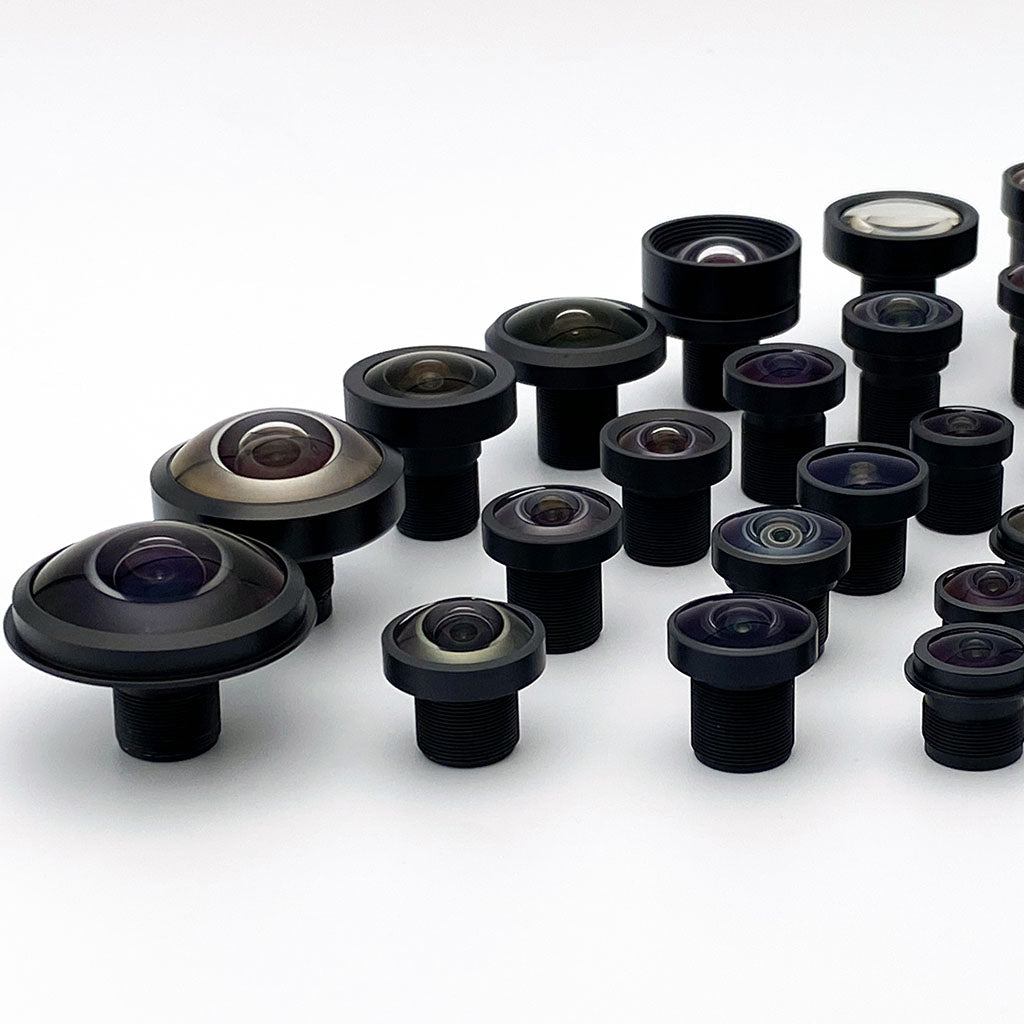

電子部品検査用マシンビジョンレンズ:PCB、半導体、およびバッテリー用途
PCB AOI, wafer and die defect detection, and battery cell and pack inspection each put different demands on the lens.

Electronics, semiconductor, and battery inspection share one framework: define the smallest feature to detect, the field of view the station needs, and the working distance the fixture allows. Then match distortion, aperture, and image circle. Low distortion serves fiducial and placement geometry, and an adjustable iris handles varying component or cell height. A longer focal length solves stand-off clearance in battery packs, while telecentric optics apply only to dimensional metrology.
Commonlands covers these tasks with the CIL052 (5.2mm M12, low distortion) and CIL522 (12mm C-mount, adjustable iris), plus the longer and large-sensor options in the products section below.
One Selection Framework for Three Inspection Domains
All three reduce to the same inputs: the smallest feature to detect reliably, the field of view to cover, and the working distance the fixture allows. Focal length then follows from focal length = (working distance × sensor dimension) / field dimension, accurate when the working distance is much larger than the focal length. Lens category comes after those numbers, not before.
| ドメイン | 代表的なタスク | 一次光学ドライバ | レンズの向き(推定) |
|---|---|---|---|
| 電子機器/プリント基板 | フィデューシャルおよび部品配置のAOI | 全周にわたって低歪み | 5mm M12 または 6~12mm Cマウント |
| 電子機器/プリント基板 | はんだ接合部/コネクタの高さ | 被写界深度を調整できる絞り | アイリスリング付きCマウント |
| 半導体 | ウェハー表面/ダイの欠陥検出 | 解像度、コントラスト、適合イメージサークル | 16~35mm Cマウント、12~20MPセンサー |
| 半導体 | Trace width and in-plane dimensional metrology | 倍率の不変性 | テレセントリック(Commonlands社製品ではありません) |
| バッテリー | パウチ型セル/タブの位置合わせ | WDにおいて、低歪みでフラットなカバレッジを実現 | 5mm M12 または 12mm Cマウント |
| バッテリー | スタンドオフ・モジュール/パックの検査 | 安全距離から標的を射程内に収める | 50mm M12 または 25mm Cマウントの望遠レンズ |
Ground-sample distance (GSD), the size one pixel represents at the object plane, ties the three domains together. GSD equals field width divided by pixel count along that axis. See spatial resolution in machine vision for the full method.

Does PCB AOI Need a Low Distortion Lens?
Yes, for most PCB geometry and fiducial tasks. AOI registers a board to fiducial marks, then measures component placement against those references, and distortion displaces apparent feature position most at the field edges, where many components sit.
A lens with 1% radial distortion, referenced to maximum image height, displaces a corner feature by about 1% of the corner field radius. On a 60mm × 45mm field the half-diagonal is 37.5mm, so the corner error is roughly 0.4mm.
A 0.4mm shift is larger than the placement tolerance most fine-pitch parts allow: an 0402 chip is only 1.0mm x 0.5mm, and 0.5mm-pitch BGA is less forgiving still. IPC-A-610 does define side-overhang limits, but as a fraction of terminal or land width that changes with package, acceptance class, and revision, so pull the criterion for your class instead of carrying one number across boards.
A lens at 0.3% TV distortion or lower is a common target for fine-pitch spacing, though the right figure depends on component pitch, field size, and the AOI system's own tolerance. The same requirement carries to code reading, since a barcode near a distorted corner has stretched elements that degrade decode confidence. See what is a low-distortion lens. Where the task is solder paste coverage or presence by silhouette, contrast matters more than geometry.
Why Does Solder Joint Inspection Put Pressure on Depth of Field?
A populated PCB is not flat. Tall connectors, through-hole components, and uneven solder volumes create height variation across the inspection area, often several millimeters on a dense board. Depth of field at a given aperture may not cover that range when focus is set to the board surface, leaving tall components or connector pins soft.
Stopping down from F/2.8 to F/8 deepens depth of field substantially at the cost of roughly three stops of light. Model the exact gain in the depth of field calculator. LED illumination in an electronics station is typically programmatic, so trading light for depth of field is practical. That trade holds only up to the diffraction limit: the Airy disk is roughly 2.44 × wavelength × F#, about 11μm at F/8. As F# climbs further, that softening grows continuously, so on small pixels added depth increasingly trades against resolution.
The iris ring on a Commonlands C-mount lens makes that trade available in the field. A fixed-aperture M12 lens does not, so its depth of field is engineered in at the design stage, through working distance and focal length. For bare boards or flat substrates the constraint never bites. Verify it with the depth-of-field calculator before committing to a fixed aperture on a board with tall components.
Choosing Between M12 and C-mount for Electronics Inspection
C-mount lenses are larger and heavier than M12. The payoff is an adjustable iris, a larger image circle, and consistent quality across a wider sensor area. A 20MP sensor on a 1.1-inch format only helps if the image circle covers it, and the Commonlands CIL544 25mm C-mount carries a 17.6mm image circle for exactly that.
When M12 Still Makes Sense
M12 is the right default when the head must fit a tight fixture and the sensor is 1/1.8 inch or smaller. Pick-and-place machines, label applicators, and inline conveyors often build the camera into the machine body, where C-mount diameter will not fit. The Commonlands CIL052 5.2mm M12 lens, at −0.1% distortion and covering up to 1/1.8-inch sensors, holds low distortion in a compact housing. Fixed aperture is fine for presence, polarity, or code reading on near-flat boards.
Choosing a Machine Vision Lens for Semiconductor Inspection
Semiconductor inspection covers wafer surface screening for particles and process defects, die inspection of bond pads and alignment marks, and package inspection of solder ball geometry or lead coplanarity. It starts from the same three inputs as electronics inspection, but feature sizes are typically an order of magnitude finer, which tightens the resolution and distortion budgets.
The task splits into two categories. Defect detection flags anomalies and does not need the image to represent physical dimensions, so catalog distortion in the 0.3% to 0.5% range is usually tolerable because contrast and resolution drive detection. Dimensional metrology measures trace width, die placement, or bump height to a tolerance, and there the figures often quoted, below 0.1% or below 0.05% for critical dimensions, are screening thresholds rather than an accuracy specification.
Read those percentages carefully. A catalog figure is nominal and uncalibrated, quoted against one metric (TV or optical/rectilinear) at one reference field height, so two lenses at the same number are not interchangeable. What governs dimensional accuracy is the residual left after calibration and how stable it is across temperature, refocus, and unit-to-unit spread. Budget the measurement, then use catalog distortion to shortlist.
GSD sizes resolution here as it does for PCB work: 2 to 3 times smaller than the minimum feature is a common starting point, with contrast, MTF, and noise setting the exact ratio. The Commonlands CIL533 and CIL535 are specified at −0.1% distortion and the CIL545 at −0.07%. Treat those as shortlisting figures, not accuracy claims.
Framing the same field from farther back with a longer lens narrows the spread of viewing angles across the field, so the specular condition changes less from center to edge. That is a perspective and pupil-geometry effect, not something focal length delivers on its own, and it does not remove glare: where a highlight lands is set by the illumination direction against the surface normal. Fix the lighting geometry first, then use the longer standoff to make what is left uniform.
Choosing a Machine Vision Lens for Battery Inspection
Battery inspection spans pouch cell and prismatic case surface inspection, cylindrical cell code reading, weld and seal verification at cell tabs, and stand-off inspection of modules and packs. The first three follow the electronics-inspection framework. The fourth introduces mechanical clearance that keeps the camera away from the target.
Flat Cell Surfaces and Code Reading
Pouch cells and prismatic cases are flat targets viewed roughly overhead, so the low-distortion logic from PCB fiducials applies: barrel distortion bows straight edges outward and shifts tab positions radially inward, and the resulting position error must be checked against the measurement tolerance. A distortion percentage without a convention and field height cannot establish that tolerance. Code reading needs its own sampling and decoding tests.
Weld and seal inspection is the exception, caring about contrast at the weld zone more than geometry, since coaxial or structured illumination is the driving factor.
Why Stand-off Inspection Needs a Longer Focal Length
Battery module and pack assemblies have thermal components, structural members, and wiring that block close camera placement, often forcing the camera outside a 200mm to 500mm exclusion zone. A longer focal length reaches a narrow field of view from that distance without wide-angle distortion. The Commonlands 50mm M12 CIL051 (9° FoV, 0.1% TV distortion) is the telephoto pick for a connector or localized mark, where a 12mm lens at the same distance would cover far too wide a field.
When a Telecentric Lens Is Justified Across All Three Domains
Object-space telecentric lenses keep the chief ray close to parallel with the optical axis (the entrance pupil sits at infinity), so an object's apparent size stays effectively constant as its distance from the lens varies within the depth of field. It rarely helps pass/fail detection, unless perspective-driven changes in apparent size or occlusion sway the classification.
Trace width, pad pitch, and tab spacing require a calibrated relationship between pixel positions and object coordinates. Bump height and lead coplanarity need a depth-sensitive method such as triangulation, stereo, focus scanning, or interferometry. A standard entocentric lens introduces an apparent position error that grows with off-axis angle and with how far the feature sits from the calibrated plane.
On a flat, well-fixtured target that error is largely absorbed by calibration, and entocentric optics measure it fine. Telecentricity is justified when height variation and perspective would otherwise push the in-plane measurement error beyond the allowed tolerance.
Elsewhere, compare the practical benefit with the added size and cost. A telecentric lens needs a front element at least as large as the object field, so a lens covering a 50mm zone is at least 50mm across at the front, which constrains fixture design and costs far more than a comparable C-mount lens. PCB AOI, wafer and die defect detection, code reading, and weld inspection are pass/fail tasks a well-specified C-mount lens handles without that penalty.
Commonlands does not currently offer telecentric lenses. For dimensional metrology that genuinely requires them, verify the object-field size and depth-of-field specification against the measurement tolerance before committing. See what is a telecentric lens for the underlying optics and lenses for quality inspection for the broader framework this pillar sits under.
Top Machine Vision Lenses for Electronics Inspection
These fixed-focal-length lenses cover the pass/fail and low-distortion measurement tiers for PCB, semiconductor, and battery inspection. Each has published distortion and image circle figures. None has autofocus. This table is a set of examples, not the full catalog.
| 検査対象領域 | レンズ | マウント | EFL | この選手を選んだ理由 |
|---|---|---|---|---|
| PCBのフィデューシャルおよび配置のAOI | CIL052 | M12 | 5.2mm | −0.1% distortion holds component positions across the field. 70° FoV at a 7.2mm circle, and the 9.0mm as-designed circle covers up to 1/1.8″ sensors in a compact head. |
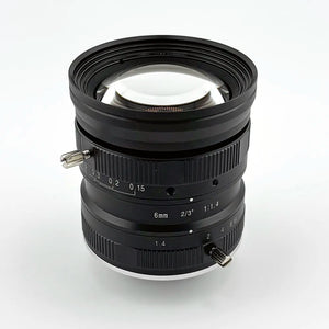
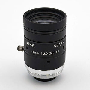
| はんだ接合部およびコネクタの検査 | CIL522 | Cマウント | 12mm | F/1.4 adjustable iris trades light for depth of field across board height variation. 51° FoV at an 11mm image circle for 2/3″ sensors. |
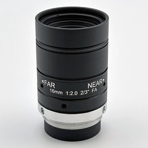
| ウェーハ表面+基板のAOI | CIL533 | Cマウント | 16mm | −0.1% distortion and an 11mm image circle for 2/3″ 12MP sensors. Resolution and uniformity for surface defect screening. |
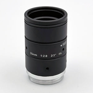
| ダイの検査+位置合わせ | CIL535 / CIL545 | Cマウント | 35mm | Higher magnification at longer working distance. CIL535 holds −0.1% distortion on a 2/3″ 11mm circle (18° field), CIL545 tightens to −0.07% on a 1.1″ 17.6mm circle for the metrology edge. |
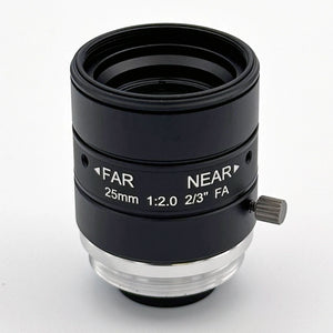
| 大型センサー搭載の20MP+検査 | CIL544 | Cマウント | 25mm | 17.6mm image circle covers 1.1″ 20MP+ sensors. F/1.8 adjustable iris and 130mm–∞ working distance. |
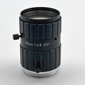
| バッテリーモジュール+パックのスタンドオフ | CIL051 | M12 | 50mm | 9° FoV reaches the target across a 200–500mm clearance zone. 0.1% TV distortion at a 7.5mm reference circle. |


よくある質問
マシンビジョンによる電子部品の検査には、どのようなレンズを使用すべきでしょうか?
Start with the task, not the lens family. PCB AOI and fiducial checks need low distortion, and solder and connector inspection needs an adjustable iris for depth of field. High-resolution stations need an image circle matched to the sensor. Commonlands picks include the CIL052 (5.2mm M12), CIL522 (12mm C-mount), and CIL544 (25mm C-mount, large-sensor).
ウェーハやダイの検査において、どの程度の歪みが許容範囲となるのでしょうか?
It depends on the task. For defect detection, many teams tolerate 0.3% to 0.5% distortion or more, since the goal is flagging anomalies. Metrology work is usually screened at below 0.1%, or below 0.05% for critical dimensions, but those are shortlisting thresholds against a stated metric and field position, not accuracy specifications: the real figure follows the calibrated residual, its stability, and the measurement error budget. Commonlands C-mount lenses such as the CIL535 (−0.1%) and CIL545 (−0.07%) are common starting points for AOI and alignment.
スタンドオフ方式のバッテリー検査では、なぜより長い焦点距離が必要なのでしょうか?
Battery module and pack assemblies have clearances, thermal management components, and structural members that keep the camera back. A longer focal length, typically 25mm to 50mm in M12 or C-mount format, reaches a narrow field of view from a greater working distance without wide-angle distortion. See machine vision lens for long working distance for the full guide.
PCB、半導体、またはバッテリーの検査には、テレセントリック光学系が必要ですか?
Telecentric optics are useful when changes in magnification or perspective would exceed the task tolerance. That can include dimensional measurement, defect classification, assembly checks, and feature matching. A single 2D telecentric view does not measure height by itself. Commonlands does not currently offer telecentric lenses.
電子機器検査ステーションの焦点距離はどのように選べばよいですか?
Use focal length = (working distance × sensor dimension) / field dimension, accurate when the working distance is much larger than the focal length. At a 200mm working distance, a 7.2mm sensor width, and a 100mm wide field, that gives 14.4mm, so a 12mm lens fits with margin. Verify with the field-of-view calculator and EFL calculator.
Need Help Selecting a Lens for an Inspection Station?
Send your working distance, sensor format, and inspection task (PCB, wafer, die, or battery cell and pack) to the Commonlands engineering team. We will confirm distortion, iris, and image circle requirements and recommend the right optic. Commonlands lenses are MTF characterized, and orders placed before 12 PM PST ship the same day.